09/12/2007
Peaking
inside an organic transistor
Recent Research from the group of Professor Xiaoyang Zhu.
Charge transport at or across interfaces is central
to the operation of a wide variety of molecule-based devices, including
organic light-emitting diodes, organic thin film transistors (OTFT), organic
photovoltaic cells. In each of these devices, the critical charge transporting
interfaces are buried interfaces,
which are not readily accessible to conventional structural or spectroscopic
probes. Though there have been tremendous advancements in molecule-based
electronics in the last a few years, the difficulty in determining structure-property
relationships at buried interfaces has produced a knowledge gap that is
a key obstacle to future development. Gaining rigorous and verifiable knowledge
of the molecular states involved during the build up and movement of charge
would help to close that gap.
A recent JACS paper by graduate student Loren
Kaake, postdoc Ying Zou, and chemistry professor Xiaoyang Zhu, in collaboration
with Dr. Matt Panzer and Prof. Dan Frisbie of Chemical Engineering & Materials
Science, demonstrated an exciting approach to probe buried interfaces (http://pubs.acs.org/cgi-bin/abstract.cgi/jacsat/2007/129/i25/abs/ja070615x.html).
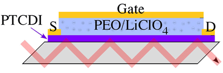
These authors applied attenuated-total-internal-reflection
Fourier transform infrared (ATR-FTIR) spectroscopy to directly probe
active layers in organic thin film transistors (OTFTs) fabricated on top
of IR waveguides. The OTFT studied uses the n-type organic semiconductor,
N-Nfdioctyl-3,4,9,10-perylene tetracarboxylic diimide (PTCDI-C8) and a
polymer electrolyte gate dielectric made from polyethylene oxide (PEO)
and LiClO4. FTIR spectroscopy of the device shows signatures
of anionic PTCDI-C8 species and broad polaron bands when the organic semiconductor
layer is doped under positive gate bias (VG).
The authors discovered two distinctive doping regions: a reversible and
electrostatic doping region for VG
2V and an irreversible and electrochemical
doping regime for VG > 2V. Based on intensity loss of vibrational peaks
attributed to neutral PTCDI-C8, the authors reported a quantitative charge
carrier density of 2.9x10¹⁴/cm2 at VG = 2 V; this charge injection density corresponded
to the conversion of slightly over one monolayer of PTCDI-C8 molecules
into anions. At higher gate bias voltage, electrochemical doping involving
the intercalation of Li+ into the organic semiconductor film
was found to convert all PTCDI-C8 molecules in a 30 nm film into anionic
species. For comparison, when a conventional gate dielectric (polystyrene)
was used, the maximum charge carrier density achievable at VG
= 200 V was ~4.5x10¹³/cm2, which
corresponds to the conversion of 18% of a monolayer of PTCDI-C8 molecules
into anions. The success of this study opened the door to exciting research
opportunities in quantitative study of organic electronics.
|