
Tip Localized Transient Absorption
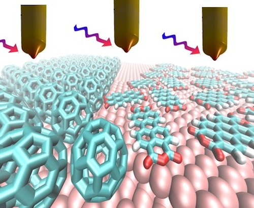
Understanding the dynamics of excitons and excited state charges is important for developing next generation photovoltaics and photocatalysts. However, these dynamics can depend sensitively on their local environment, and we need new techniques for correlating structure and dynamics at the molecular length scale. Our lab is develop new instrumentation to investigate the dynamics and heterogeneities of charge and optical excitations in 2D materials and at interfaces. Because of reduced charge screening in 2D, monolayer based systems are more prone to extended perturbations to both the optical and electronic properties from point defects, chemical adsorbates, and atmospheric adsorbates. We will develop ultrafast tip enhanced fluorescence, and correlate the resulting dynamics to atomically resolved structures and electronic structures in an ultrahigh vacuum scanning tunneling microscope. These results will provide new insight into the properties of 2D materials which will aid the subsequent development of 2D photonics, optical detectors, photovoltaics, and 2D optical based sensors.
Buried Interfaces and Instrisic Properties of 2D Materials
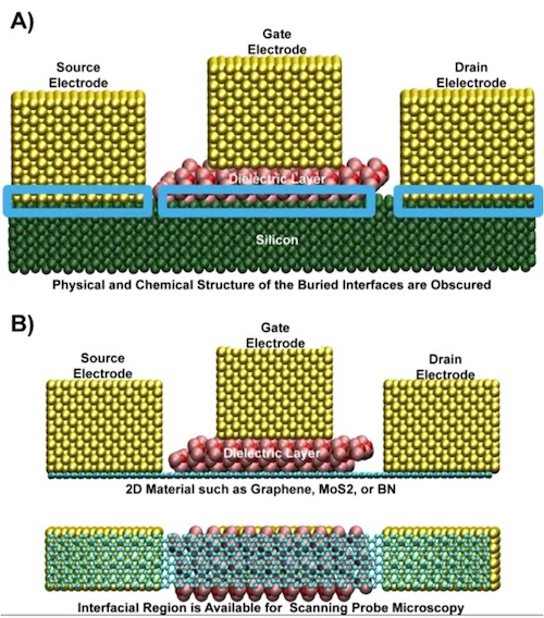
We are exploiting the 2D nature of new monolayer based electronic materials such as graphene and MoS2 to study the chemistry of reactions commonly used to build electronic devices. Typically, the deposition of metal electrodes and other hierarchical chemistries used to create layered devices also create a buried chemical interface. In 3D materials, this interfacial region may or may not play an important role in device performance because charges can circumvent it by movement in the third dimension. In 2D materials, however, this interfacial layer should directly impact device performance, and will significantly perturb the local physical and chemical environment. We will probe the local physical and chemical environment of 2D materials before and after chemistry common to device fabrication. By suspending these materials, we will be able to perform chemistry on a single side, as normally happens in device processing, but still be able to access the interface by scanning tunneling microscopy. The results from this project could significantly impact the field of device fabrication of all forms, both in two and three dimensions.
Epitaxial and CVD Growth of New Materials
Our lab is developing the chemistry needed to create highly crystalline, large area monolayers of metal chalcogenides starting with MoS2. Unlike graphene, monolayer MoS2 is a direct band gap semiconductor, and recent progress has been made improving is electrical performance and characterizing its optical properties. We will grow wafer scale, monolayer MoS2 via thermal evaporation and chemical vapor deposition on single crystal wafers of 4H- SiC. By characterizing his growth process using scanning probe and optical techniques, not only will my group aim to create an electronically and commercially relevant 2D material, but we will also better understand the chemistry and physics of the growth process. This knowledge will guide further attempts to grow new monolayer based materials for electronic and optical applications.